Buck Regulator Calculator
Estimate duty cycle, inductor value, ripple current, output capacitance, input capacitor RMS current, and thermal load for step-down DC converter design.
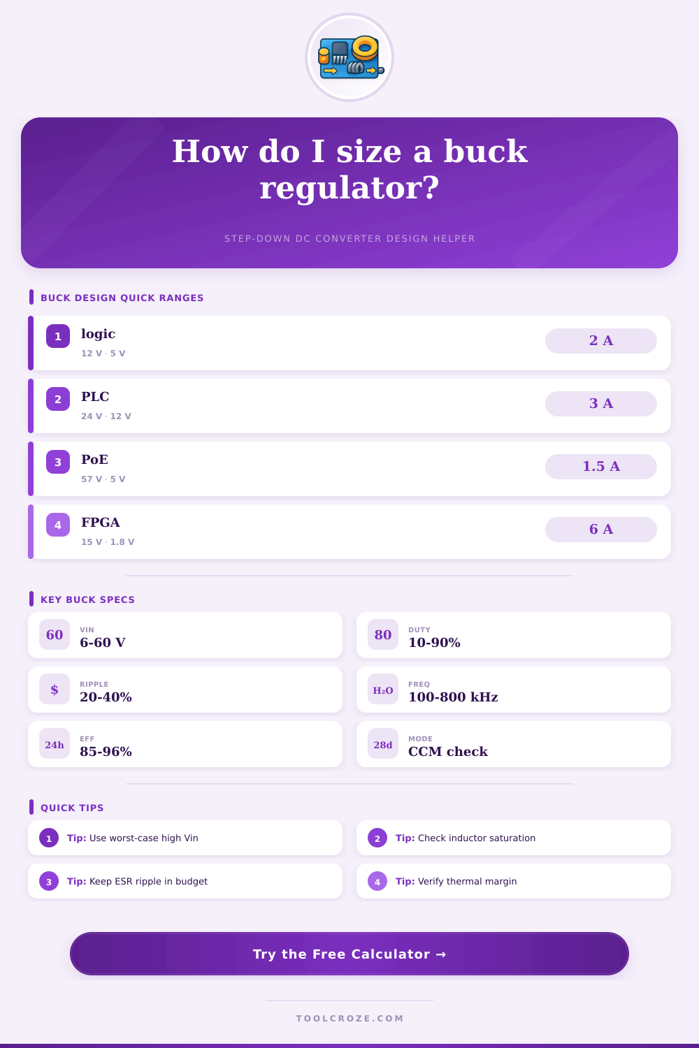
Choose a real converter scenario, then adjust the electrical limits for your controller, switch, diode, and capacitor family.
Calculated Buck Converter Design
| Design Target | Conservative Range | Typical Range | Design Note |
|---|---|---|---|
| Inductor ripple current | 15% to 25% of Iout | 25% to 40% of Iout | Lower ripple improves output ripple but raises inductance size. |
| Switching frequency | 100 kHz to 250 kHz | 300 kHz to 800 kHz | Higher frequency shrinks L and C but raises switching loss. |
| Duty cycle operating window | 15% to 85% | 20% to 80% | Very low or high duty cycles can stress minimum on or off time limits. |
| Output ripple voltage | 0.5% to 1% of Vout | 1% to 2% of Vout | Noise-sensitive analog loads often need post filtering. |
| Capacitor Type | Useful Strength | Ripple Concern | Common Buck Placement |
|---|---|---|---|
| MLCC ceramic | Low ESR and high frequency bypassing | DC bias reduces effective capacitance | Near switch input and output pins |
| Polymer electrolytic | High ripple current with stable ESR | Larger footprint than ceramics | Output bulk reservoir |
| Aluminum electrolytic | High bulk capacitance for load steps | ESR and temperature aging | Input bus and lower frequency bulk |
| Tantalum polymer | Compact bulk capacitance | Surge and derating requirements | Output rail where derating is verified |
| Rectifier Style | Drop Model | Efficiency Impact | Best Fit |
|---|---|---|---|
| Schottky diode buck | 0.25 V to 0.6 V forward drop | Simple but lossy at high current | Low current rails and rugged prototypes |
| Synchronous MOSFET buck | Iout multiplied by Rds(on) | Better at low output voltage | High current 5 V, 3.3 V, and core rails |
| Integrated regulator module | Vendor efficiency curve | Thermal limited by package and PCB | Fast design where datasheet limits dominate |
| Controller with external FETs | FET loss plus gate charge | Scales well for high current designs | Custom industrial, telecom, and FPGA rails |
| Application Rail | Typical Input | Common Output | Component Emphasis |
|---|---|---|---|
| Automotive sensor rail | 9 V to 16 V nominal | 5 V at 0.5 A to 2 A | Transient voltage rating and EMI filtering |
| Industrial control rail | 18 V to 36 V bus | 12 V or 5 V at 1 A to 5 A | Thermal rise, surge margin, and field wiring spikes |
| PoE powered device | 37 V to 57 V isolated front end | 12 V, 5 V, or 3.3 V | High step-down ratio and controller voltage rating |
| FPGA or processor core | 5 V to 15 V intermediate bus | 0.8 V to 1.8 V high current | Transient response, low ESR output bank, and remote sense |
A buck regulator are a device that takes energy from one voltage rail and moves it to another voltage rail by chopping the voltage of the input rail to a lower output voltage. When chopping the input voltage of a buck regulator, the converter must decide how much energy to allow through to the load and how much energy to discard. A buck regulator that is incorrecty size will run hot, ring, or fail under the required load for the application.
Using a tool to visualize these relationship is more useful than using the datasheet table for the regulator alone. The first decision to make in the design of a buck regulator is the amount of ripple current that is allowed to pass through the inductor. By reducing the percentage of the ripple current, the output voltage will be quiet and have less stress placed upon the capacitors that are placed downstream of the load.
How to Design a Buck Regulator
However, utilizing a lower percentage for the ripple current will require the use of a larger inductor. Utilizing a higher percentage for ripple current will allow for the inductor to be smaller in size, but will require the capacitor to handle the higher AC component of the output current. These calculations can be performed with the calculator provided here.
It is important to ensure that the peak current is within the saturation limit for the selected inductor, as well as ensuring that the RMS current is within the temperature limit for the input capacitor. Switching frequency is another major factor in the design of a buck regulator. Higher switching frequency allow for the inductor and the output capacitor to be smaller.
However, higher switching frequencies will increase the switching loss in the power devices of the regulator, as well as make it more difficult to control the voltage spikes that can be created by the layout inductance of the circuit layout. Many regulator controllers will have a minimum on-time for the switching frequency of the devices. This minimum on-time is more difficultly to satisfy at a lower duty cycle (higher output voltage relative to the input) for the load.
Thus, you can perform calculations at two different switching frequencies to compare how the inductor value can be reduced by increasing the switching frequency and how the input capacitor RMS current can be affected by changing the switching frequency and duty cycle. The duty cycle for a buck regulator is the ratio of the output voltage to the input voltage. The actual duty cycle that is used for the regulator devices will be slightly less than the ideal duty cycle due to the voltage drops of the switches and the diode.
The calculator performs these calculations automaticly. The calculator will display the actual duty cycle next to the ideal duty cycle so that the designer can be aware that the regulator devices may be operating close to their minimum on-time or off-time limits. Running at or near these limits will cause the regulator to either have poor transient response characteristics or may even operate in discontinuous conduction mode at light load.
Output capacitance is determined by the ripple current and the allowable voltage excursion for the output capacitor. This value is the minimum required to achieve the ripple current at the output capacitor. Real designs will require additional capacitance to account for the ESR of the capacitors, the layout inductance of the circuit, and the dynamic requirement of the load.
Thus, this value is only the floor for the output capacitors required for an application, and not the actual value that will be needed. Additionally, the ESR limit of the capacitors has to also be evaluated for this ripple current, especially if using ceramic capacitors where the effective capacitance can drop at high DC bias. Input capacitor stress is another consideration in the design of the buck regulator.
Excessive stress on the input capacitor can lead to the regulator emitting electromagnetic radiation that can interfere with other circuits or component on the same circuit board, or can lead to overheating of the capacitor. The RMS current through the input capacitor is equal to the output current multiplied by the square root of the duty cycle times one minus the duty cycle. The RMS current will be the highest at a duty cycle of 50%.
Many intermediate bus dc/dc buck regulators will have a duty cycle near 50%. Thus, it is important to calculate the RMS current for the input capacitor at the highest input voltage to determine whether a single ceramic capacitor can be used or if a polymer electrolytic capacitor will be required to handle the ripple current at the input. Efficiency will impact the design decision in two major ways, in regard to the input current that will be drawn from the upstream dc power supply, and in regard to the total amount of power that must be dissipated as heat in the buck converter devices.
You can enter the efficiency into the calculator to determine the input current and the power loss in the devices. The power loss that is calculated is only as accurate as the efficiency estimate, but will allow for at least a rough estimate of the thermal requirement of the regulator. The efficiency will impact the size of the regulator; high efficiency will permit the use of a smaller device.
In many instances, the thermal considerations will impact the design decision of the regulator, forcing either the reduction in switching frequency to reduce the power loss in the devices or the use of a synchronous rectifier instead of a diode in the circuit. Real designs for buck regulators will incorporate factors that a calculator could not possibly envision. Factors such as the source impedance that exists in the input circuit due to the wiring or the connectors to the dc power supply will create an input voltage that may be outside of the limits that were entered into the calculator.
Load transients may require more additional input capacitance than those calculated by the ripple current. Additionally, as the regulator devices heat during operation, the inductor may reach its saturation current, as well as the ESR of the output capacitors may increase. Therefore, a design that passes through the calculator must be tested in the laboratory to verify that it will perform as expected.
One of the most common mistake in the design is treating the initial calculation as the final answer. If any of the parameters for the design are changed, such as the switching frequency or the ripple percentage, the other parameters will change as well. For instance, altering the ripple percentage will alter the inductor value, peak current, and capacitor RMS current.
Thus, the calculations must be performed multiple times with different parameter value to determine which parameters are sensitive to alteration and which are robust to changes in those parameters. Once all of the relationship between the parameters of the buck regulator have been established, the calculated values for each of the parameters will be translated to real components. Each component will have a datasheet that includes information about how the components behave within the regulator and under different loads.
The calculator is a tool that shortens the initial pass through the design of a buck regulator, allowing for more time to be spent considering the second-order and third-order effect of the design. These second-order and third-order effect will determine whether the buck regulator will run cool and quiet under the loads that are applied to it.